 |
|
2D and 3D Board Viewers
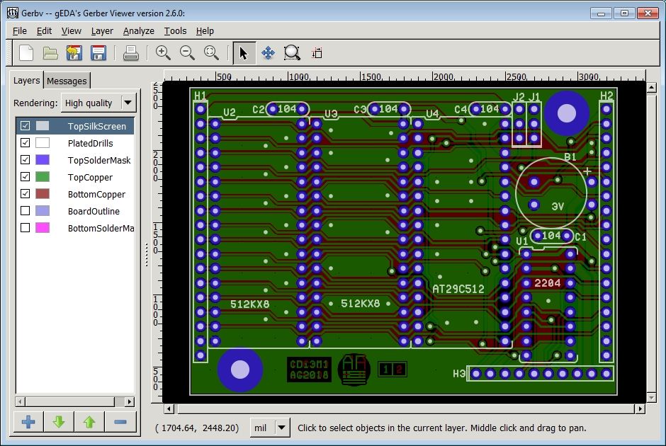
- Part of the gplEDA project, Gerbv is a pretty good 2D Gerber viewer, click on the picture on the left below to see an example Gerbv screen. Gerbv projects are supplied as zipped archives, the user extracts archive contents in a folder of choice and double-clicks on the file with *.gvp extension to start the utility. Gerbv can be downloaded and installed from here: https://sourceforge.net/projects/gerbv/. After installation you might want to try this sample, and if so click to download the GERBV.CDi3M1.zip project.
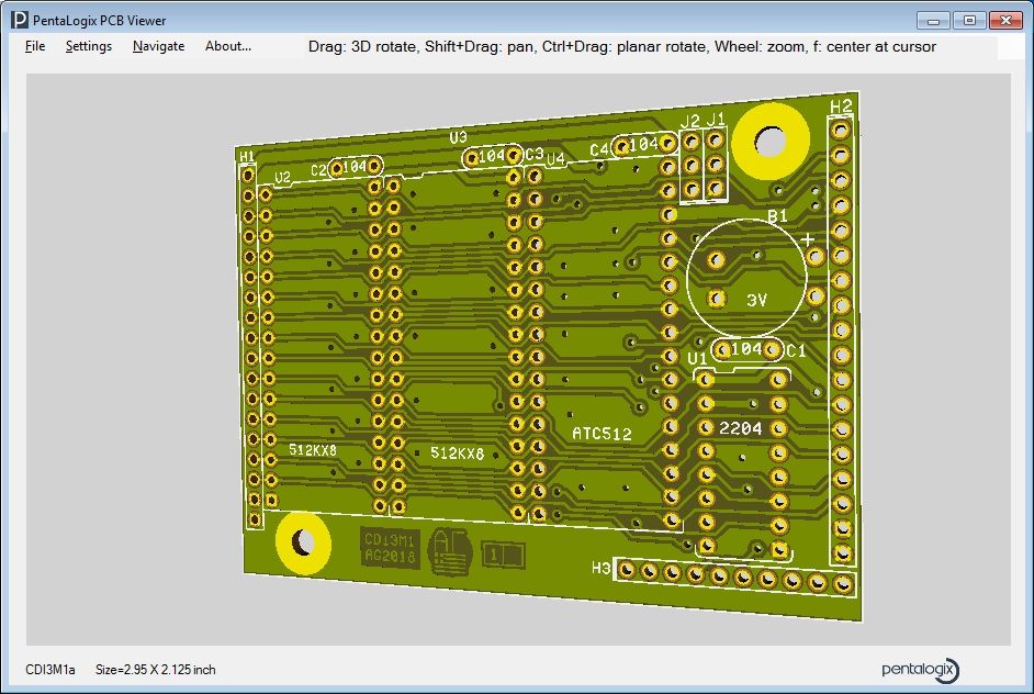
- Part of the Pentalogix CAM software suite Viewmate, 3D Board Viewer provides much more realistic output of what the physical board will look like, particularly useful before the design files are sent out to manufacture. The viewer runs on Windows Vista and above and exists as both 32-bit and 64-bit versions. 3D board projects are supplied as zipped archives, however, no extraction is necessary as the utility opens *.zip archives. The 32-bit installer is here, ftp://ftp.pentalogix.com/Updates/3DBoardViewer/ and the 64-bit version is here, ftp://ftp.pentalogix.com/Updates/3DBoardViewer64/. Once installed the utility can open 3D *.zip archives like this 3D edition of the same board.
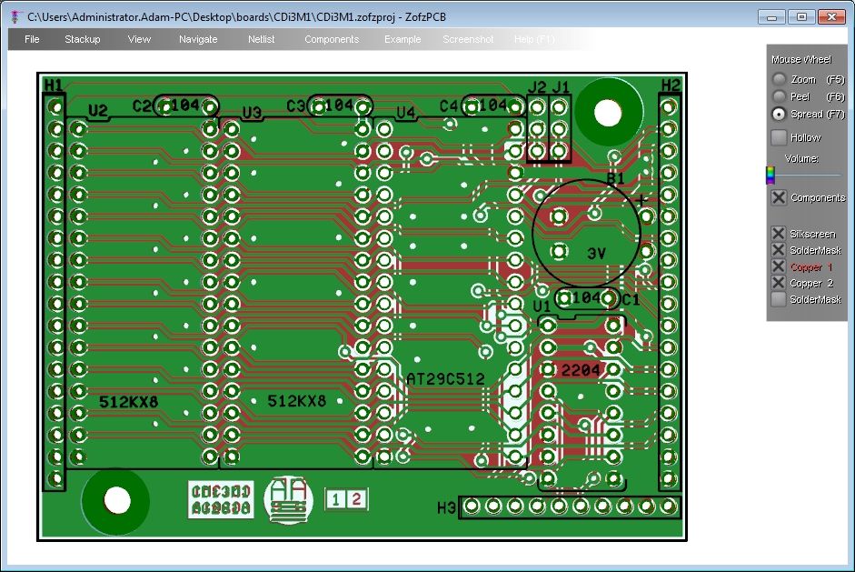
- ZofzPCB is a promising 3D viewer, in development for about a year or so. There are 2 files to every project, a stackup file with extension *.camset and a project file with extension *.zofzproj. The utility can be downloaded from the zofzPCB website: https://www.zofzpcb.com/. As above, the same sample board is represented in this *.zip archive.
- In the remainder of this page the 2D icon you see below represents a 2D Gerbv project and the 3D icon represents a 3D Board Viewer project, all three icons are links to project design files. The filenames of the archives indicate the utility they are intended for, so "GERBV", "3D", and "3DZ" mean 2D Gerbv project, 3D Board Viewer project, and 3D zofzPCB project respectively.
2015-2018 - CDi4 Boards
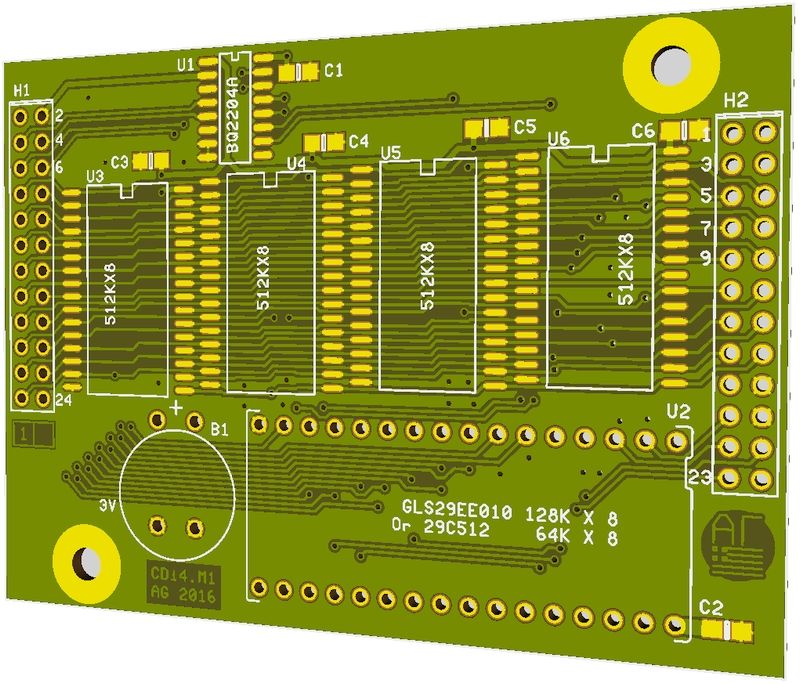
2016 - CDi4.M1 Storage Memory/EEPROM Board
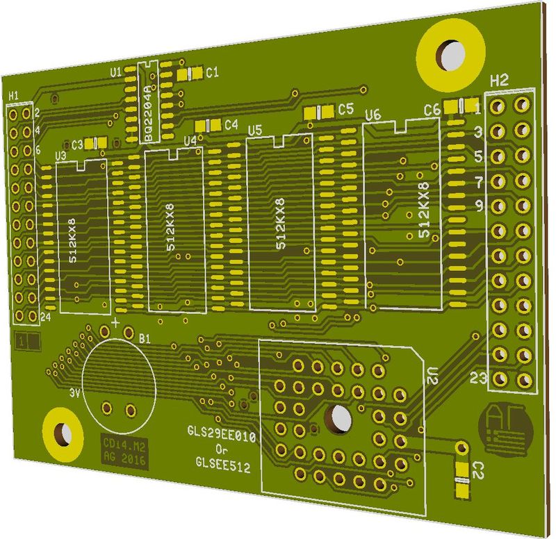
2016 - CDi4.M2 Storage Memory/EEPROM Board
- Board status: designed June 2016, not built yet.
- Doubles the CDi3 storage Static RAM, SRAM, to 2 Mbytes.
- Accommodates 64k x 8 and 128k x 8 EEPROMS in 32-pin DIP packages.
- Board pdf: layers combined, board pdf: layers on separate pages.
2016 CDi4M1


- Board status: designed June 2016, not built yet.
- Doubles the CDi3 storage Static RAM, SRAM, to 2 Mbytes.
- Accommodates 64k x 8 and 128k x 8 EEPROMS in PLCC packages.
- Board pdf: layers combined, board pdf: layers on separate pages.
2016 CDi4M2
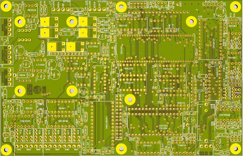
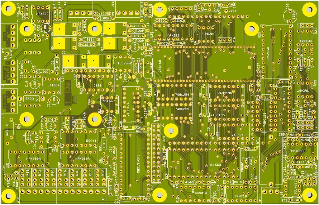
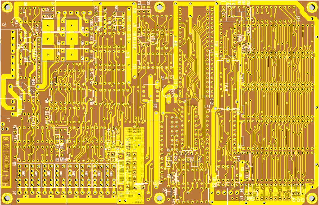
2016 - CDi3.P7 Main Board - One More Step Closer to CDi4
- Clock increase from 6.144MHz to 7.373MHz resulting in a maximum baud rate of 115.2K for both communication channels.
- Ability to use the newer DS1553 RTC, since the DS1386 is now obsolete but still available in the aftermarket.
- Design preserves the original 8-channel analog circuitry, multiplexer is not used in digital modes, ADC only there to read the battery voltage.
- Added a Bluetooth wireless interface to the main communications channel.
- The CDi4 will be built as a general purpose industrial class controller as per lake Erie roadmap, the CDi4 is extremely unlikely to ever be used in the lake.
- Board status: designed in April 2016, built in June 2016.
- Board compatible with obsolete DS1386-8 RTC and 28-pin DS1553 RTC.
- Supports serial RS232, RS485, and Bluetooth wireless interfaces.
- Z8S180 64-pin DIP, Dual In-line Package, commercial temperature only, 0C to 70C.
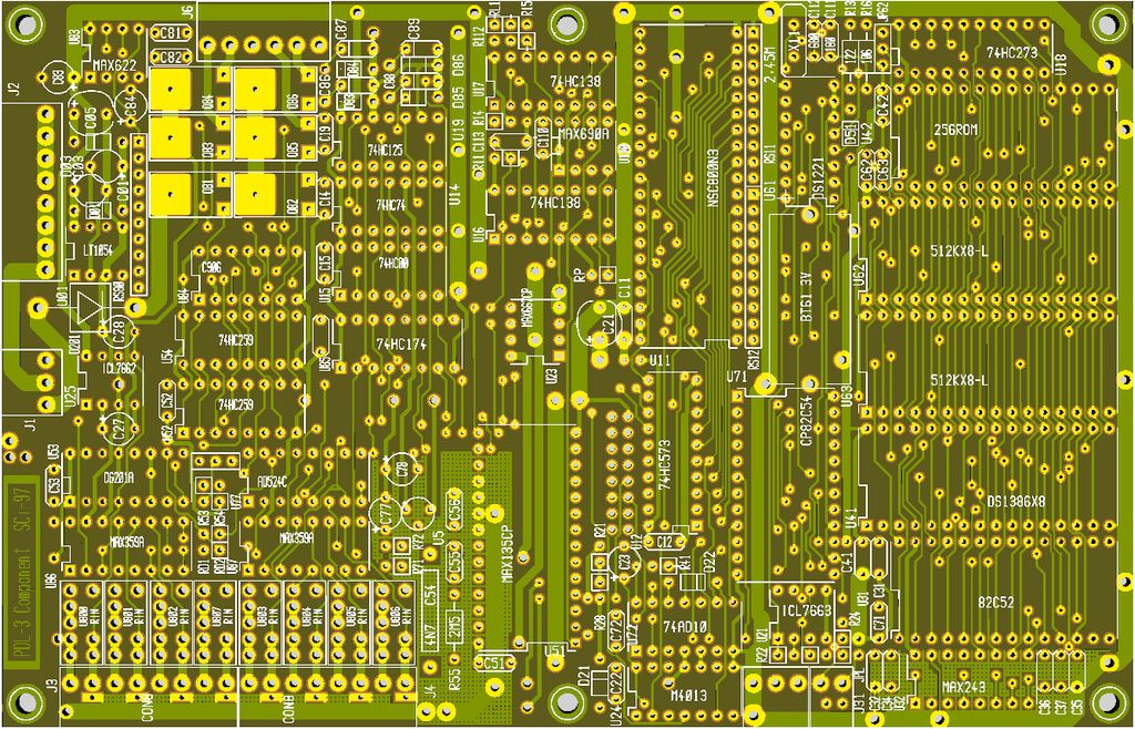
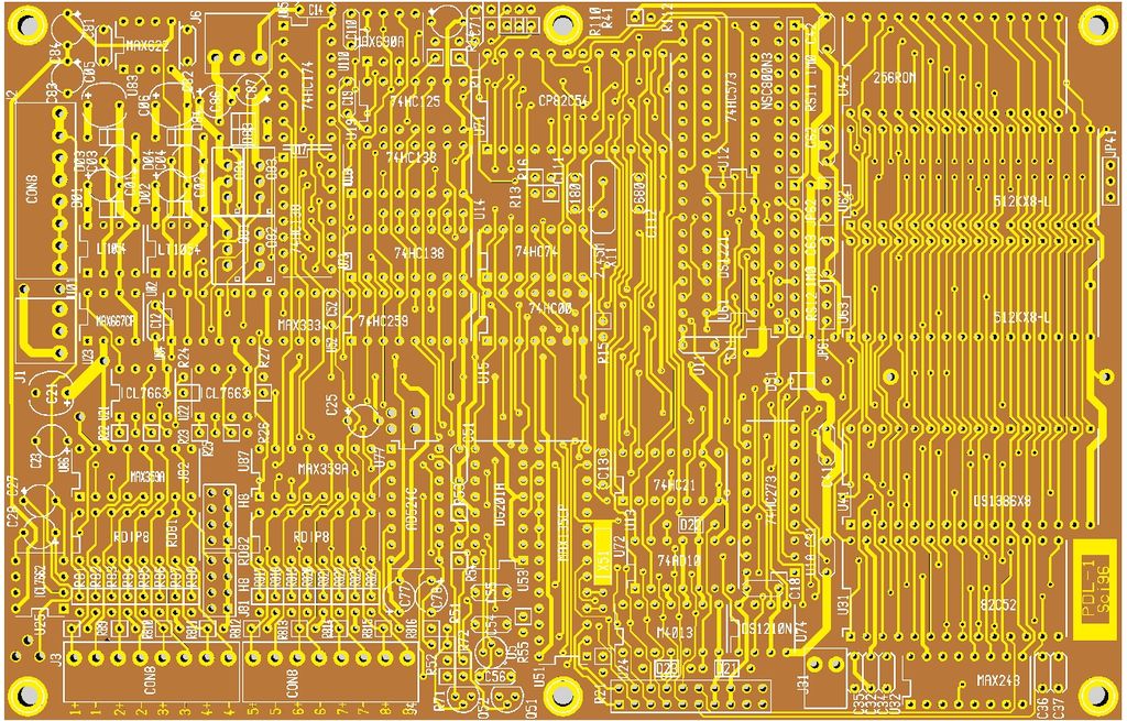
2016 CDi3.P7
- Physical board top copper layer and bottom copper layer.
- Board pdf: layers combined, board pdf: layers on separate pages.
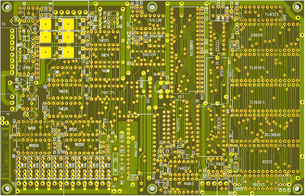
2016 - CDi3.LE Main Board - One Step Closer to CDi4
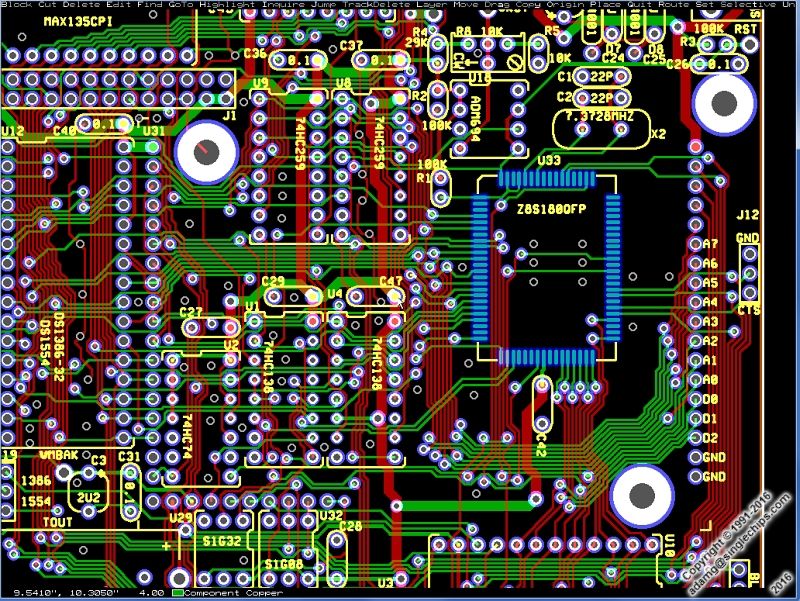
- Board status: designed in May 2016, not built yet.
- Board compatible with obsolete DS1386-32 and current DS1554 RTCs, but not compatible with 28-pin DS1553 RTC.
- Supports serial RS485 and Bluetooth wireless interfaces.
- Z8S180 80-pin QFP, Quad Flat Pack, commercial or industrial temperature, 0C to 70C or -40C to +105C.
- Board pdf: layers combined, board pdf: layers on separate pages.
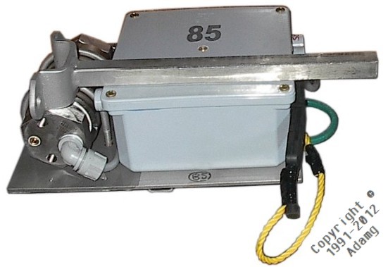
2016 - RS485 Board for the ZDL5
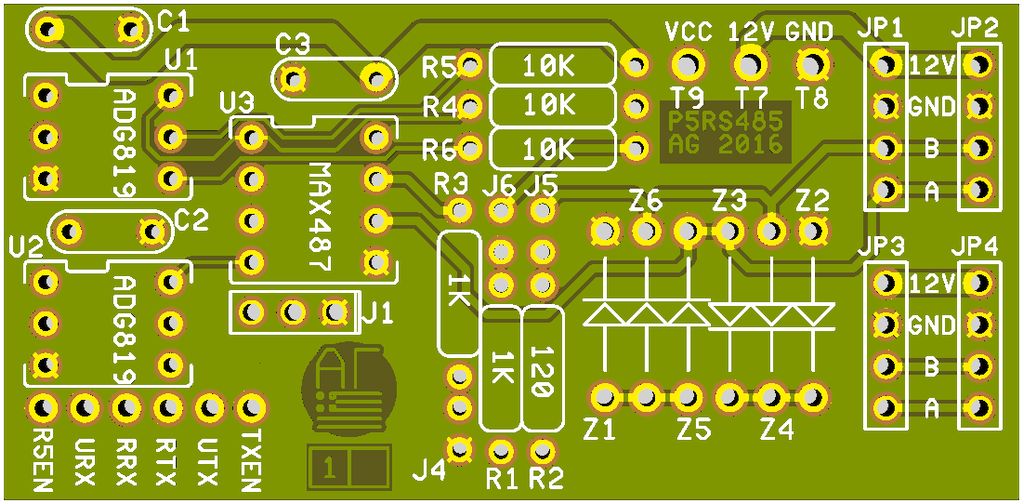
- The board was designed after the ZDL5 prototype was built, its purpose is to make the transformation of an analogue PDL5 into a digital ZDL5 easier.
P5RS485
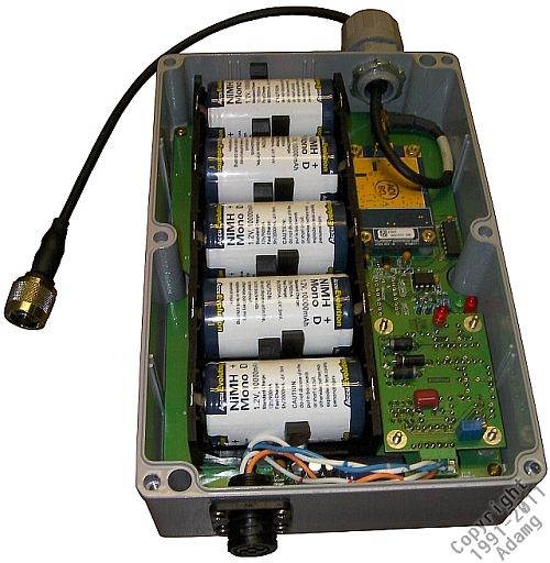
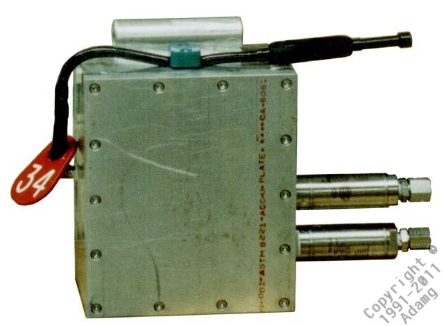
2010 - XTMASTER
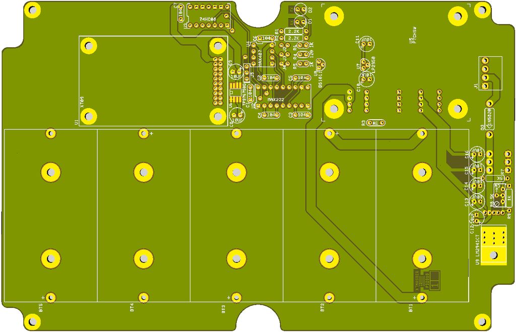
2010 - P7MAIN, Charger and Memory Boards - On the Way to CDi4
|
CPU
|
Clock
|
Heartbeat |
On Time
|
Memory
|
Solenoids
|
Max. Baud
|
|
Z8S180
|
3.07MHz
|
2 Secs
|
3 Secs
|
1MB
|
2
|
38400
|
2010 Memory
2010 Charger
2010 P7MAIN
2000 - Now - CDi2 Boardsets
1999 - 2006 - PDL5/CDi1
|
CPU
|
Clock
|
Heartbeat |
On Time
|
Memory
|
Solenoids
|
Max. Baud
|
|
NSC800N
|
3.07MHz
|
5 Secs
|
6 Secs
|
1MB
|
2
|
38400
|
P5
1998 - PDL4
|
CPU
|
Clock
|
Heartbeat |
On Time
|
Memory
|
Solenoids
|
Max. Baud
|
|
NSC800N
|
1.2MHz
|
10 Secs
|
11 Secs
|
1MB
|
2
|
9600
|
P4
1997 - PDL3
|
CPU
|
Clock
|
Heartbeat |
On Time
|
Memory
|
Solenoids
|
Max. Baud
|
|
NSC800N
|
1.2MHz
|
10 Secs
|
11 Secs
|
1MB
|
2
|
9600
|
P3
1996 - PDL1
|
CPU
|
Clock
|
Heartbeat |
On Time
|
Memory
|
Solenoids
|
Max. Baud
|
|
NSC800N
|
1.2MHz
|
10 Secs
|
11 Secs
|
256KB
|
1
|
9600
|
P1
Contact: